|
|
| (같은 사용자의 중간 판 9개는 보이지 않습니다) |
| 1번째 줄: |
1번째 줄: |
| − | SAW-핸드폰DPX | + | SAW 듀플렉서 |
| | + | <ol> |
| | + | <li> [[전자부품]] |
| | <ol> | | <ol> |
| | <li> [[SAW대문]] | | <li> [[SAW대문]] |
| | + | <li> [[듀플렉서]] |
| | + | <ol> |
| | + | <li> [[SAW 듀플렉서]] - 이 페이지 |
| | + | <ol> |
| | + | <li> [[9.5x7.5 SAW 듀플렉서]] |
| | + | <li> [[5.0x5.0 SAW 듀플렉서]] |
| | + | <li> [[3.8x3.8 SAW 듀플렉서]] |
| | + | <li> [[3.2x2.5 SAW 듀플렉서]] |
| | + | <li> [[3.0x2.5 SAW 듀플렉서]] |
| | + | <li> [[2.5x2.0 SAW 듀플렉서]] |
| | + | <li> [[2.0x1.6 SAW 듀플렉서]] |
| | + | <li> [[1.8x1.4 SAW 듀플렉서]] |
| | + | <li> [[1.55x1.15 SAW 듀플렉서]] |
| | + | <li> [[1.4x1.1 SAW 듀플렉서]] |
| | + | </ol> |
| | + | <li>참고 |
| | + | <ol> |
| | + | <li> [[FEMiD]] |
| | + | <li> [[PAM]] |
| | + | <li> [[PAMiD]] |
| | + | </ol> |
| | + | </ol> |
| | + | <li>참고 |
| | <ol> | | <ol> |
| − | <li> [[SAW-핸드폰DPX]] - 이 페이지 | + | <li> [[필터 정격전력]] 내전력, 허용전력 |
| − | <li> [[세라믹필터]] | + | </ol> |
| − | <li> [[유전체필터]]
| |
| − | <li> [[SAW-CLP]]
| |
| − | <li>
| |
| | </ol> | | </ol> |
| | <li>필터 두 개로 듀플렉서를 만듬 | | <li>필터 두 개로 듀플렉서를 만듬 |
| 21번째 줄: |
43번째 줄: |
| | image:u_100_017.jpg | Tx, Rx필터로 duplexer 만드는 법 | | image:u_100_017.jpg | Tx, Rx필터로 duplexer 만드는 법 |
| | </gallery> | | </gallery> |
| − | </ol>
| |
| − | <li>3.0x3.0mm 필터를 사용함.
| |
| − | <ol>
| |
| − | <li>삼성전기, 개발품(?) 모델명 모름
| |
| − | <ol>
| |
| − | <li>이 상태로 있길래
| |
| − | <gallery>
| |
| − | image:saw_dpx9575_02_001.jpg
| |
| − | image:saw_dpx9575_02_002.png
| |
| − | image:saw_dpx9575_02_003.jpg
| |
| − | </gallery>
| |
| − | <li>깡통을 벗기니
| |
| − | <gallery>
| |
| − | image:saw_dpx9575_02_004.jpg
| |
| − | </gallery>
| |
| − | <li>3.0x3.0mm 쏘필터를 다시 납땜해서
| |
| − | <gallery>
| |
| − | image:saw_dpx9575_02_005.jpg | 왼쪽 881, 오른쪽 836
| |
| − | image:saw_dpx9575_02_006.png
| |
| − | </gallery>
| |
| − | <li>쏘필터 뚜껑을 벗기니
| |
| − | <gallery>
| |
| − | image:saw_dpx9575_02_007.jpg
| |
| − | image:saw_dpx9575_02_008.jpg | 왼쪽 881, 오른쪽 836
| |
| − | image:saw_dpx9575_02_009.jpg | X881 50
| |
| − | image:saw_dpx9575_02_010.jpg | X836 50
| |
| − | image:saw_dpx9575_02_011.jpg
| |
| − | </gallery>
| |
| − | </ol>
| |
| − | </ol>
| |
| − | </ol>
| |
| − | <li>9.5x7.5mm
| |
| − | <ol>
| |
| − | <li>후지쯔(Fujitsu Media Devices Limited), FAR-D5CC-881M50-D1A4
| |
| − | <ol>
| |
| − | <li>제품규격서 - 12p
| |
| − | <li> [[StarTAC]] 휴대폰에서
| |
| − | <gallery>
| |
| − | image:startac01_002.jpg | B면
| |
| − | image:startac01_006.jpg | [[PAM]] [[커플러]]
| |
| − | image:startac01_005.jpg | 아래:ANT, 왼쪽:Tx, 오른쪽:Rx
| |
| − | image:startac01_007.jpg
| |
| − | </gallery>
| |
| − | </ol>
| |
| − | <li>삼성전기 X836KP - 2001년 제품
| |
| − | <ol>
| |
| − | <li>자재 및 공정
| |
| − | <ol>
| |
| − | <li>사용 패키지와 리드(8.0x6.0mm) 비교
| |
| − | <gallery>
| |
| − | image:lid_ausn10_005.jpg
| |
| − | image:lid_ausn10_006.jpg
| |
| − | image:lid_ausn10_007.jpg
| |
| − | </gallery>
| |
| − | <li>융착 결과 - AuSn 두께가 30um으로 두꺼워야 하는 이유. 패키지가 크면 warpage가 커, 빈공간을 메워야 하므로
| |
| − | <gallery>
| |
| − | image:lid_ausn10_008.jpg
| |
| − | image:lid_ausn10_009.jpg
| |
| − | </gallery>
| |
| − | </ol>
| |
| − | <li>2017년 [[Redmi Note 4X]] 휴대폰에서 나온 1.8x1.4mm 및 1.55x1.15mm 크기와 비교
| |
| − | <gallery>
| |
| − | image:saw_dpx9575_02_012.jpg | 9.5x7.5mm vs 1.8x1.4mm
| |
| − | image:saw_dpx9575_02_013.jpg | 9.5x7.5mm vs 1.55x1.15mm
| |
| − | </gallery>
| |
| − | <li>[[포켓WiFi]]에서 사용된 2.0x1.6mm 제품과 비교하기 위해 분해
| |
| − | <ol>
| |
| − | <li>비교 사진
| |
| − | <gallery>
| |
| − | image:saw_dpx9575_01_001.jpg
| |
| − | image:saw_dpx9575_01_002.jpg
| |
| − | image:saw_dpx9575_01_003.jpg
| |
| − | image:saw_dpx9575_01_004.jpg
| |
| − | image:saw_dpx9575_01_005.jpg
| |
| − | </gallery>
| |
| − | <li>칩 전체
| |
| − | <gallery>
| |
| − | image:saw_dpx9575_01_006.jpg | Rx(881.5MHz)
| |
| − | image:saw_dpx9575_01_007.jpg | Tx(836.5MHz)
| |
| − | </gallery>
| |
| − | <li>확대
| |
| − | <gallery>
| |
| − | image:saw_dpx9575_01_008.jpg
| |
| − | image:saw_dpx9575_01_009.jpg
| |
| − | </gallery>
| |
| − | <li>더 확대
| |
| − | <gallery>
| |
| − | image:saw_dpx9575_01_010.jpg | 주기: 4.27um - Rx(881.5MHz)
| |
| − | image:saw_dpx9575_01_011.jpg | 위쪽 주기: 4.56um - Tx(836.5MHz)
| |
| − | </gallery>
| |
| − | <li>무라타 2016과 비교
| |
| − | <gallery>
| |
| − | image:saw_dpx9575_01_012.jpg
| |
| − | image:saw_dpx9575_01_013.jpg
| |
| − | </gallery>
| |
| − | <li>Rx 칩에서, HWP 폰트(유니코드 문자코드 263B, Black Smiling Face)로 만든 패턴인듯.
| |
| − | <gallery>
| |
| − | image:saw_dpx9575_01_014.jpg
| |
| − | </gallery>
| |
| − | </ol>
| |
| − | </ol>
| |
| − | </ol>
| |
| − | <li>5.0x5.0mm
| |
| − | <li>3.8x3.8mm
| |
| − | <ol>
| |
| − | <li>SAWTEK 856331, CDMA용 850MHz
| |
| − | <ol>
| |
| − | <li>규격서 - 6p
| |
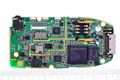
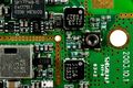
| − | <li> Motorola [[MS500]] 휴대폰에서
| |
| − | <ol>
| |
| − | <li>세트에서. W마크가 이 기종이다. 1997년 141일차, 생산지C
| |
| − | <gallery>
| |
| − | image:ms500_01_026.jpg
| |
| − | </gallery>
| |
| − | <li>주파수 특성
| |
| − | <gallery>
| |
| − | image:ms500_01_027.jpg
| |
| − | image:ms500_01_027_001.png | 광대역 특성
| |
| − | image:ms500_01_027_002.png | 통과대역 특성
| |
| − | image:ms500_01_027_003.png | 3포트 반사 특성
| |
| − | image:ms500_01_027_004.png | 3포트 매칭
| |
| − | image:ms500_01_027_005.png | Tx/Rx ladder 필터의 지연시간 약 20nsec
| |
| − | </gallery>
| |
| − | <li>뚜껑 열기
| |
| − | <gallery>
| |
| − | image:ms500_01_028.jpg | 와이어본딩이 L로 동작하므로 정교하게 연결한다.
| |
| − | image:ms500_01_029.jpg | 두 패턴 사이에 Y자 접지 패턴이 이채롭다.
| |
| − | </gallery>
| |
| − | <li>패턴
| |
| − | <gallery>
| |
| − | image:ms500_01_030.jpg | 위쪽이 Tx 패턴일 듯
| |
| − | image:ms500_01_031.jpg | [[정전기]] 파괴
| |
| − | image:ms500_01_032.jpg | 정전기 파괴
| |
| − | image:ms500_01_033.jpg | 글꼴 설계, M자는 [[Copyright]]
| |
| − | </gallery>
| |
| − | </ol>
| |
| − | </ol>
| |
| − | </ol>
| |
| − | <li>3.2x2.5mm
| |
| − | <ol>
| |
| − | <li>무라타 SAW UMTS 2100(Tx 1920-1980, Rx 2110-2170) DPX, 3.2x2.5mm LTCC 구리전극 캐비티, 2칩, 플립본딩, AuSn 실링
| |
| − | <ol>
| |
| − | <li> [[LG-SH170]] 에서
| |
| − | <ol>
| |
| − | <li>리드 실링이 틀어져 있다. (힘들게 하나씩 리드를 누르면서 실링했다는 뜻)
| |
| − | <gallery>
| |
| − | image:sh170_052.jpg
| |
| − | image:sh170_053.jpg
| |
| − | image:sh170_054.jpg
| |
| − | </gallery>
| |
| − | <li>AuSn 실링
| |
| − | <gallery>
| |
| − | image:sh170_055.jpg
| |
| − | image:sh170_056.jpg | 검정색 칩, 이젝트핀 자국
| |
| − | image:sh170_057.jpg
| |
| − | image:sh170_058.jpg | 기판 구리전극이 뜯어졌다. 칩에서 보호막 두께가 달라 색상이 달리 보인다.
| |
| − | </gallery>
| |
| − | <li>칩 패턴
| |
| − | <gallery>
| |
| − | image:sh170_059.jpg
| |
| − | image:sh170_060.jpg
| |
| − | image:sh170_061.jpg
| |
| − | image:sh170_062.jpg | 융착온도 때문에 금속 확산
| |
| − | </gallery>
| |
| − | <li>어떤 칩 다이싱 단면
| |
| − | <gallery>
| |
| − | image:sh170_063.jpg | 한쪽면
| |
| − | image:sh170_064.jpg | 같은 칩에서 그 반대 한쪽면
| |
| − | image:sh170_065.jpg
| |
| − | </gallery>
| |
| − | </ol>
| |
| − | <li> [[SPH-W4700]]
| |
| − | <ol>
| |
| − | <li>외관
| |
| − | <gallery>
| |
| − | image:w4700_020.jpg
| |
| − | image:w4700_021.jpg
| |
| − | </gallery>
| |
| − | <li>플립 본딩
| |
| − | <gallery>
| |
| − | image:w4700_022.jpg | 검정색 칩, 이젝트핀 자국
| |
| − | image:w4700_023.jpg
| |
| − | image:w4700_024.jpg | LTCC 구리전극 캐비티
| |
| − | </gallery>
| |
| − | <li>칩1, 유전체 보호막 때문에 웨이퍼 표면이 보라색으로 보임
| |
| − | <gallery>
| |
| − | image:w4700_025.jpg | W734-A1
| |
| − | </gallery>
| |
| − | <li>칩2, 유전체 보호막 때문에 웨이퍼 표면이 보라색으로 보임
| |
| − | <gallery>
| |
| − | image:w4700_026.jpg
| |
| − | </gallery>
| |
| − | </ol>
| |
| − | </ol>
| |
| − | </ol>
| |
| − | <li>2.5x2.0mm
| |
| − | <ol>
| |
| − | <li>세트에서 발견
| |
| − | <ol>
| |
| − | <li>와이솔, 핸드폰 GT-B6520에서
| |
| − | <gallery>
| |
| − | image:gt_b6520_012.jpg | SAW 부품 1,2,3,4,5,6 위치
| |
| − | image:gt_b6520_016.jpg | 2 듀플렉서 칩 두께가 서로 다르다.
| |
| − | image:gt_b6520_016_001.jpg | XG50PD5-MP6 Rx HJD
| |
| − | image:gt_b6520_016_002.jpg | XG50PD5-MP? Tx HJD
| |
| − | </gallery>
| |
| − | <li> [[3G통신모듈]]에서
| |
| − | <ol>
| |
| − | <li>한국 비트앤펄스(bits and pulse) 회사에서 제작한 BPW-M100모듈
| |
| − | <ol>
| |
| − | <li>통신모듈
| |
| − | <gallery>
| |
| − | image:3g_module01_014.jpg | RF 면
| |
| − | image:3g_module01_025.jpg | QSC6240
| |
| − | </gallery>
| |
| − | <li>외관
| |
| − | <gallery>
| |
| − | image:3g_module01_017.jpg
| |
| − | image:3g_module01_018.jpg
| |
| − | </gallery>
| |
| − | <li>에폭시를 제거하면
| |
| − | <gallery>
| |
| − | image:saw_dpx2520_01_001.jpg | Rx, Tx
| |
| − | image:saw_dpx2520_01_002.jpg | Tx 칩이 더 얇다. 먼저 본딩했다.
| |
| − | </gallery>
| |
| − | <li>칩 뜯는 방법
| |
| − | <gallery>
| |
| − | image:saw_dpx2520_01_003.jpg | 위로 올라가지 않게 위에서 누른다.
| |
| − | image:saw_dpx2520_01_004.jpg | 칼날을 밀어 넣기 전
| |
| − | image:saw_dpx2520_01_005.jpg | 칼날을 밀어 넣은 후
| |
| − | </gallery>
| |
| − | <li>패키지와 칩. Tx칩은 큰 내전력이 요구되므로, Rx칩과 공정이 달라, 표면 구조가 다르기 때문에 다른 빛깔로 관찰된다.
| |
| − | <gallery>
| |
| − | image:saw_dpx2520_01_006.jpg
| |
| − | </gallery>
| |
| − | <li>Rx 칩. 아래 중앙이 Ant, 아래 좌우가 diffential out(좌우 대칭)
| |
| − | <gallery>
| |
| − | image:saw_dpx2520_01_007.jpg | 왼쪽 육교 패턴 일부는 높아서, 칼에 의해 잘린 흔적이 보인다.
| |
| − | image:saw_dpx2520_01_011.jpg
| |
| − | image:saw_dpx2520_01_012.jpg
| |
| − | image:saw_dpx2520_01_013.jpg
| |
| − | image:saw_dpx2520_01_015.jpg | 정렬키와 (갈색)보호막
| |
| − | </gallery>
| |
| − | <li>Tx 칩
| |
| − | <gallery>
| |
| − | image:saw_dpx2520_01_008.jpg | Tx
| |
| − | image:saw_dpx2520_01_008_001.png | 1폴 공진기로 등가회로
| |
| − | image:saw_dpx2520_01_009.jpg
| |
| − | image:saw_dpx2520_01_010.jpg
| |
| − | image:saw_dpx2520_01_014.jpg | probing 바늘 자국. 밀리지 않아 거의 원형이다.
| |
| − | </gallery>
| |
| − | </ol>
| |
| − | <li>CDMA 1x EV-DO USB Modem
| |
| − | <ol>
| |
| − | <li>외관
| |
| − | <gallery>
| |
| − | image:3g_module03_003.jpg
| |
| − | image:3g_module03_003_017.png
| |
| − | image:3g_module03_003_001.jpg
| |
| − | </gallery>
| |
| − | <li>Duplexer, 836/881MHz, 2.5x2.0mm
| |
| − | <gallery>
| |
| − | image:3g_module03_003_008.jpg
| |
| − | image:3g_module03_003_009.jpg
| |
| − | image:3g_module03_003_010.jpg
| |
| − | image:3g_module03_003_011.jpg
| |
| − | image:3g_module03_003_012.jpg
| |
| − | image:3g_module03_003_014.jpg | Tx필터 813077C AC
| |
| − | image:3g_module03_003_015.jpg | Rx필터 813256
| |
| − | image:3g_module03_003_016.jpg | 정전기 방지용, 저항 쇼트 패턴
| |
| − | </gallery>
| |
| − | </ol>
| |
| − | </ol>
| |
| − | </ol>
| |
| − | </ol>
| |
| − | <li>2.0x1.6mm
| |
| − | <ol>
| |
| − | <li>한국 SK텔레콤용 [[포켓WiFi]]에서 사용된 무라타 850/1800MHz
| |
| − | <ol>
| |
| − | <li>2.0x1.6mm 1800MHz용
| |
| − | <ol>
| |
| − | <li>외형
| |
| − | <gallery>
| |
| − | image:mobile_router01_017.jpg
| |
| − | </gallery>
| |
| − | <li>내부
| |
| − | <gallery>
| |
| − | image:mobile_router01_017_001.jpg | 왼쪽 Tx, 오른쪽 Rx
| |
| − | image:mobile_router01_017_002.jpg | Rx 아래 - 밸런스 출력
| |
| − | </gallery>
| |
| − | <li>Rx 칩
| |
| − | <gallery>
| |
| − | image:mobile_router01_017_003.jpg
| |
| − | image:mobile_router01_017_004.jpg
| |
| − | image:mobile_router01_017_005.jpg
| |
| − | image:mobile_router01_017_006.jpg | interdigitated C(IDT C)
| |
| − | image:mobile_router01_017_007.jpg | 절연
| |
| − | image:mobile_router01_017_008.jpg
| |
| − | </gallery>
| |
| − | <li>Tx 칩에서
| |
| − | <gallery>
| |
| − | image:mobile_router01_017_009.jpg
| |
| − | image:mobile_router01_017_010.jpg
| |
| − | </gallery>
| |
| − | <li>칩에서 범프볼(와이어가 길게 존재함)
| |
| − | <ol>
| |
| − | </ol><gallery>
| |
| − | image:mobile_router01_017_011.jpg
| |
| − | </gallery>
| |
| − | <li>2.0x1.6mm 850MHz용
| |
| − | <ol>
| |
| − | <li>외형
| |
| − | <gallery>
| |
| − | image:mobile_router01_018.jpg
| |
| − | </gallery>
| |
| − | <li>Rx 칩
| |
| − | <gallery>
| |
| − | image:saw_dpx2016_01_001.jpg
| |
| − | image:saw_dpx2016_01_003.jpg
| |
| − | image:saw_dpx2016_01_007.jpg
| |
| − | </gallery>
| |
| − | <li>Tx 칩
| |
| − | <gallery>
| |
| − | image:saw_dpx2016_01_002.jpg
| |
| − | image:saw_dpx2016_01_004.jpg
| |
| − | image:saw_dpx2016_01_005.jpg
| |
| − | image:saw_dpx2016_01_006.jpg
| |
| − | </gallery>
| |
| − | </ol>
| |
| − | </ol>
| |
| − | </ol>
| |
| − | <li>1.8x1.4mm
| |
| − | <ol>
| |
| − | <li>2017년 [[Redmi Note 4X]] 휴대폰에서 나온 Taiyo Yuden 1.8x1.4mm
| |
| − | <gallery>
| |
| − | image:saw_dpx9575_02_012.jpg | 9.5x7.5mm vs 1.8x1.4mm
| |
| − | </gallery>
| |
| − | <li> Xiaomi [[Redmi Note 4X]] 휴대폰에서, 7개 사용하는데,
| |
| − | <ol>
| |
| − | <li>Qorvo , TQQ1003 1747.5/1842.5MHz LTE Band3 WLP [[SMR]]-[BAW]] 참조
| |
| − | <li>Murata 1.55x1.15mm 한 개 (아래 참조)
| |
| − | <li>Taiyo Yuden 5개 - 1개 FBAR+SAW조합, 1개 사파이어접합, 3개 SAW
| |
| − | <ol>
| |
| − | <li>주파수를 알아내기 위한 간이 측정 방법
| |
| − | <gallery>
| |
| − | image:redmi_note4x_188.jpg
| |
| − | </gallery>
| |
| − | <li>측면
| |
| − | <gallery>
| |
| − | image:redmi_note4x_188_001.jpg | 두께가 다르다.
| |
| − | image:redmi_note4x_188_002.jpg | 금속이 세라믹보다 두꺼운 이유는 세라믹을 자른 후 도금을 했기 때문에다.
| |
| − | image:redmi_note4x_188_003.jpg | 잘린 세라믹 측면에 도금을 위해 연결된 전극이 보이지 않는다.
| |
| − | </gallery>
| |
| − | <li>701, LTE Band7 Tx:2535MHz, Rx:2655MHz
| |
| − | <ol>
| |
| − | <li>주파수 파형
| |
| − | <gallery>
| |
| − | image:redmi_note4x_189.png | 2535MHz
| |
| − | </gallery>
| |
| − | <li>Tx필터 온도 특성 실험-1
| |
| − | <ol>
| |
| − | <li>치구 준비
| |
| − | <gallery>
| |
| − | image:redmi_note4x_189_001.jpg | 정확한 주파수 특성 그래프를 위해서 접지 납땜을 추가함
| |
| − | image:redmi_note4x_189_001_001.png | 주파수 특성 그래프
| |
| − | </gallery>
| |
| − | <li>가열 냄비 준비
| |
| − | <gallery>
| |
| − | image:redmi_note4x_189_002.jpg
| |
| − | image:redmi_note4x_189_003.jpg
| |
| − | </gallery>
| |
| − | <li>Fluorinert 액체는 Solvay Solexis회사의 GALDEN D03 제품(비점 190도, 유전율 2.1, 유전손실 0.0002)을 부었다.
| |
| − | <gallery>
| |
| − | image:redmi_note4x_189_004.jpg | Fluorinert 액체를 부어도 파형에는 큰 변화가 없다.
| |
| − | image:redmi_note4x_189_005.jpg | 온도센서를 설치하고 Fluorinert를 부은 후,
| |
| − | image:redmi_note4x_189_006.jpg
| |
| − | image:redmi_note4x_189_007.jpg | 온도센서는 DMM저항값으로 읽어드림
| |
| − | </gallery>
| |
| − | <li>실험 방법
| |
| − | <gallery>
| |
| − | image:redmi_note4x_189_008.jpg | 별도의 K타입 열전대로 온도 측정 문제점을 체크함
| |
| − | image:redmi_note4x_189_009.jpg | 50도 미만에서 선풍기로 온도를 더 빨리 내림
| |
| − | </gallery>
| |
| − | <li>5071C 네트워크분석기에서 주파수 값과 3478A DMM에서 R 읽어 온도 환산 프로그램 [[tcf-ibw.txt]]
| |
| − | <li>엑셀 데이터
| |
| − | <gallery>
| |
| − | image:redmi_note4x_189_010.png | 온도프로파일
| |
| − | image:redmi_note4x_189_011.png | 피크이득
| |
| − | image:redmi_note4x_189_012.png | -10dB 중심주파수
| |
| − | image:redmi_note4x_189_013.png | -30ppm 온도계수를 갖는다.
| |
| − | image:redmi_note4x_189_014.png | 대역폭
| |
| − | </gallery>
| |
| − | </ol>
| |
| − | <li>Tx필터 온도 특성 실험-2, 첫실험이 성공이어서 온도를 더 높게 빠르게 올림
| |
| − | <ol>
| |
| − | <li>30와 130도씨에서 특성 그래프 비교
| |
| − | <gallery>
| |
| − | image:redmi_note4x_189_015.png
| |
| − | </gallery>
| |
| − | <li>그래프
| |
| − | <gallery>
| |
| − | image:redmi_note4x_189_016.png | 30~130도씨 온도프로파일
| |
| − | image:redmi_note4x_189_017.png | 피크이득
| |
| − | image:redmi_note4x_189_018.png | -10dB 중심주파수
| |
| − | image:redmi_note4x_189_019.png | -33ppm 온도계수를 갖는다.
| |
| − | image:redmi_note4x_189_020.png | 대역폭
| |
| − | </gallery>
| |
| − | <li>사용된 액체 부피가 작고, 수위가 낮아 온도 편차가 크다. 그러므로 빠른 온도 상승에서는 액체를 순환시켜야(저어야)겠다.
| |
| − | </ol>
| |
| − | <li>다이 내부 - 두께가 두꺼운 제품이다.
| |
| − | <ol>
| |
| − | <li>SAW + BAW 조합이다.
| |
| − | <gallery>
| |
| − | image:redmi_note4x_189_021.jpg
| |
| − | image:redmi_note4x_189_022.jpg | Tx는 baw 필터(레이저 다이싱)에서 F-bar, Rx는 saw 필터이다.
| |
| − | </gallery>
| |
| − | <li>F-BAR baw 필터
| |
| − | <gallery>
| |
| − | image:redmi_note4x_189_023.jpg | W868-08
| |
| − | image:redmi_note4x_189_024.jpg | 진동판에 무늬가 있는 #1~#6 표시함
| |
| − | </gallery>
| |
| − | <li>공진기 #1~#6
| |
| − | <gallery>
| |
| − | image:redmi_note4x_189_025.jpg | #1
| |
| − | image:redmi_note4x_189_026.jpg | #2
| |
| − | image:redmi_note4x_189_027.jpg | #3
| |
| − | image:redmi_note4x_189_028.jpg | #4
| |
| − | image:redmi_note4x_189_029.jpg | #5
| |
| − | image:redmi_note4x_189_030.jpg | #6
| |
| − | </gallery>
| |
| − | <li>Rx saw 필터
| |
| − | <gallery>
| |
| − | image:redmi_note4x_189_031.jpg | W1895-14
| |
| − | image:redmi_note4x_189_032.jpg | 주기:1.48um 주파수:2655M 쏘속도:3930m/sec
| |
| − | </gallery>
| |
| − | </ol>
| |
| − | </ol>
| |
| − | <li>7B1, LTE Band2, Tx:1880MHz Rx:1960MHz, 두꺼운 제품인다.
| |
| − | <ol>
| |
| − | <li>주파수 파형
| |
| − | <gallery>
| |
| − | image:redmi_note4x_190.png | 1877MHz
| |
| − | </gallery>
| |
| − | <li>땜납으로 4변에 벽을 세웠다.
| |
| − | <gallery>
| |
| − | image:redmi_note4x_190_001.jpg
| |
| − | </gallery>
| |
| − | <li>사파이어+LT(?) 접합 웨이퍼를 사용했다.
| |
| − | <gallery>
| |
| − | image:redmi_note4x_190_002.jpg | 초경에 긁히지 않는 것으로 보아 사파이어 맞다.
| |
| − | image:redmi_note4x_190_003.jpg
| |
| − | image:redmi_note4x_190_004.jpg | LT두께 20um+사파이어두께 250um, 레이저 펀칭7번, 간격 약 27um
| |
| − | </gallery>
| |
| − | <li>다이를 뜯어냄
| |
| − | <gallery>
| |
| − | image:redmi_note4x_190_005.jpg | 밀어보니, 레이저 다이싱에 문제가 있어, 사파이어가 깨진다.
| |
| − | image:redmi_note4x_190_006.jpg
| |
| − | </gallery>
| |
| − | <li>Rx
| |
| − | <gallery>
| |
| − | image:redmi_note4x_190_007.jpg | X077-22
| |
| − | image:redmi_note4x_190_008.jpg | 주기:1.98um x 1960MHz = 3880m/sec
| |
| − | </gallery>
| |
| − | <li>Tx:1880MHz
| |
| − | <ol>
| |
| − | <li>전체
| |
| − | <gallery>
| |
| − | image:redmi_note4x_190_009.jpg | X019-21
| |
| − | image:redmi_note4x_190_009_001.jpg | 배율을 달리해서 찍음. 밝고 어두움으로 전극폭이 다르다는 것을 확인하기 위해
| |
| − | </gallery>
| |
| − | <li>withdrawal weighting에서 이처럼 전극이 넓으면 reflection withdrawal weighting, 전극을 빼면 reflection withdrawal weighting이라고 부르자.
| |
| − | <gallery>
| |
| − | image:redmi_note4x_190_009_002.jpg | 굵은 전극이 궁금해서
| |
| − | image:redmi_note4x_190_010.jpg | 주기:2.10um x 1880MHz = 3950m/sec
| |
| − | image:redmi_note4x_190_010_001.jpg | 굵은 전극 형태
| |
| − | </gallery>
| |
| − | <li>90도로 배열된 C패턴
| |
| − | <gallery>
| |
| − | image:redmi_note4x_190_011.jpg
| |
| − | image:redmi_note4x_190_012.jpg
| |
| − | </gallery>
| |
| − | </ol>
| |
| − | </ol>
| |
| − | <li>7A4, LTE Band1
| |
| − | <ol>
| |
| − | <li>주파수 파형
| |
| − | <gallery>
| |
| − | image:redmi_note4x_191.png | 1950MHz
| |
| − | </gallery>
| |
| − | <li>전체
| |
| − | <gallery>
| |
| − | image:redmi_note4x_191_001.jpg
| |
| − | image:redmi_note4x_191_002.jpg
| |
| − | </gallery>
| |
| − | <li>Rx
| |
| − | <gallery>
| |
| − | image:redmi_note4x_191_003.jpg | Rx 다이, V8151-31
| |
| − | image:redmi_note4x_191_004.jpg | Rx 어느 패턴에서 주기: 1.865um 2140MHz 쏘속도 3990m/sec
| |
| − | </gallery>
| |
| − | <li>Tx
| |
| − | <gallery>
| |
| − | image:redmi_note4x_191_005.jpg | Tx 다이
| |
| − | image:redmi_note4x_191_006.jpg | Tx 어느 패턴에서 주기: 1.949um 1950MHz 쏘속도 3800m/sec
| |
| − | image:redmi_note4x_191_007.jpg | 우측 상단, 90도 돌아간 C전용 패턴에서 주기: 1.695um
| |
| − | image:redmi_note4x_191_008.jpg | 좌측 하단, 90도 돌아간 C전용 직렬 패턴에서 주기:1.65um. 굳이 직렬로 C를 만들 이유는 내전압 때문이다. (칩 위아래로만 초전이 발생되므로 길게 연결된 패턴 때문에)
| |
| − | </gallery>
| |
| − | </ol>
| |
| − | <li>7G6, LTE Band8, 두께가 얇은 제품이다.
| |
| − | <ol>
| |
| − | <li>주파수 파형
| |
| − | <gallery>
| |
| − | image:redmi_note4x_192.png | 897.5MHz
| |
| − | </gallery>
| |
| − | <li>다이 내부
| |
| − | <gallery>
| |
| − | image:redmi_note4x_192_001.jpg | 트위저로 금속 뚜껑을 누르면서 작업했는데 다이가 깨져 있다. 리드와 다이 뒷면이 붙어 있지 않다.
| |
| − | image:redmi_note4x_192_002.jpg | 풀칠
| |
| − | image:redmi_note4x_192_003.jpg | 풀칠 수
| |
| − | image:redmi_note4x_192_004.jpg | 다이 분리
| |
| − | image:redmi_note4x_192_005.jpg | 다이
| |
| − | image:redmi_note4x_192_006.jpg | Rx 다이, 주기: 4.12um 942.5MHz 3880m/sec
| |
| − | image:redmi_note4x_192_007.jpg | Tx 다이, 주기: 4.28um 897.5MHz 3840m/sec
| |
| − | </gallery>
| |
| − | </ol>
| |
| − | <li>7E4, LTE Band5
| |
| − | <ol>
| |
| − | <li>주파수 파형
| |
| − | <gallery>
| |
| − | image:redmi_note4x_193.png | 836.5MHz
| |
| − | </gallery>
| |
| − | <li>다이 내부
| |
| − | <gallery>
| |
| − | image:redmi_note4x_193_001.jpg | 다이 뒷면 밝기가 달리 보인다.
| |
| − | image:redmi_note4x_193_002.jpg | 다이를 작게 할 수 없어, 벽이 얇아졌다.
| |
| − | image:redmi_note4x_193_003.jpg
| |
| − | image:redmi_note4x_193_004.jpg | 기판 전극표면이 비교적 평탄하다.
| |
| − | image:redmi_note4x_193_005.jpg | 본딩이 쉽게 떨어진다.(그렇게 플립본딩한 듯)
| |
| − | image:redmi_note4x_193_006.jpg | Rx 881.5MHz, 주기: 4.46um (쏘속도 3930m/sec)
| |
| − | image:redmi_note4x_193_007.jpg | Tx 836.5MHz, 어느 전극에서, 윗쪽 주기 4.60um, 아래쪽 주기 4.58um (쏘속도 3850m/sec)
| |
| − | </gallery>
| |
| − | </ol>
| |
| − | </ol>
| |
| − | </ol>
| |
| − | </ol>
| |
| − | <li>1.55x1.15mm
| |
| − | <ol>
| |
| − | <li>2017년 [[Redmi Note 4X]] 휴대폰에서 나온 무라타 1.55x1.15mm
| |
| − | <gallery>
| |
| − | image:saw_dpx9575_02_013.jpg | 9.5x7.5mm vs 1.55x1.15mm
| |
| − | </gallery>
| |
| − | <li> Xiaomi [[Redmi Note 4X]] 휴대폰에서, 7개 사용하는데, 이중 무라타 하나가 해당
| |
| − | <ol>
| |
| − | <li>Murata CG/3J, 1.55x1.15mm 크기
| |
| − | <ol>
| |
| − | <li>외관
| |
| − | <gallery>
| |
| − | image:redmi_note4x_127.jpg
| |
| − | </gallery>
| |
| − | <li>패키징
| |
| − | <gallery>
| |
| − | image:redmi_note4x_127_001.jpg | 패키지 크기 1.55x1.15mm 다이 크기 1.22x0.84mm 여유 0.33mm 및 0.31mm
| |
| − | image:redmi_note4x_127_002.jpg
| |
| − | </gallery>
| |
| − | <li>다이
| |
| − | <gallery>
| |
| − | image:redmi_note4x_127_003.jpg | EK18
| |
| − | image:redmi_note4x_127_004.jpg | 주기 2.04um(2000MHz 근처 필터)
| |
| − | </gallery>
| |
| − | </ol>
| |
| | </ol> | | </ol> |
| | </ol> | | </ol> |
| | </ol> | | </ol> |